Project in brief
Context
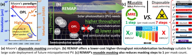
Optical projection lithography: so good, so wasteful
Today’s micro-fabrication is based on an outdated linear manufacturing logic, where most of the material, energy and monetary resources invested end up into waste streams. Considering the pervasiveness of micro-fabrication in virtually all spheres of human activities, and its impact on key enabling technologies (KETs), this economic and environmental cost is at odds with the entire United Nations’ sustainable development programme. Are we sure we can sustainably rip the benefits of today’s microfabrication paradigm for large scale applications such as photovoltaics (PV)?
Motivation
A more sustainable micro-fabrication paradigm
REMAP is a paradigm shift in micro-fabrication that combines semiconductor quality with throughput. Since (disposable) masks are a key factor to the technological success of traditional lithography, REMAP takes masks as a crucial factor into account. However, REMAP’s mask is reversible, i.e. flexible (reconfigurable on the fly) and reusable ad infinitum, enabling one-step surface patterning, which increases sustainability, in line with UN SDGs 8, 9 and 12.
Methods
Interdisciplinarity is key
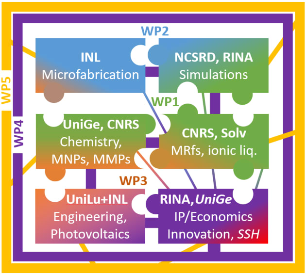
A close interaction between experts belonging to very diverse disciplines is essential to attain REMAP’s patterning breakthrough. It requires profound knowledge spanning pure and applied chemistry (organic functionalization, click-chemistry, inorganic MNPs synthesis, ionic liquids, chemical non-linearity), to soft matter physics (colloidal science, rheology and magnetic fluids). It takes state-of-the-art facilities and expertise in micro-fabrication, solid state magnetism, and electrical engineering. It involves know-how in mechanical engineering, electroplating, reactive annealing and semiconductor PV technology. It needs broad expertise in IP, in-depth knowledge of economics, business and policy, as well as soft skills on inclusive innovation and teaching strategies, including tactful talent in social sciences and humanities (SSH), like gender studies.
Expected Results
The advent of reusable masks
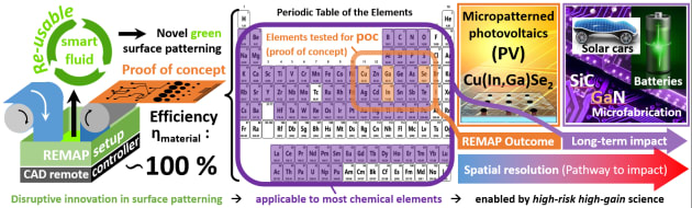
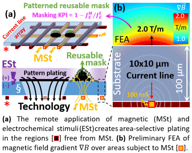
While making use of remotely (magnetically) controlled masking, REMAP creates the first reusable mask-based patterning technology by conferring plating functionality to a magnetoresponsive fluid. This crucial modification frees the system from the reliance on conventional lithography for turning masks into patterns.
REMAP overcomes the drawbacks of current masking/maskless paradigms, ferrofluids and electroplating by creating what we call magnetorheological electrolytes (MREs), composite electrolytes inspired by magnetorheological fluids (MRf), fluids that change viscosity when subject to magnetic fields. REMAP will develop a system to remotely control the microscopic shape of the MREs through microstructured magnetic fields (∇B). This revolutionises surface patterning: the spatial modulation of the field induces a contactless reversible phase split of the MRE on the substrate at the micro-scale, enabling unmasked areas to undergo selective electroplating, in the complete absence of wasteful masking or prepatterned templates.
Impact
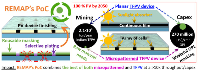
Micropatterned photovoltaic solar cells
Renewables are key to zero GHG emissions and limit global warming to 1.5°C by 2050, when PV is expected to meet > 35% of global electricity demand (= capacity of ≥ 200 GWp/a). Planar thin-film PV (TFPV) has a market size of US$ 30 Billion by 2024, is ca. 50% more energy efficient compared to silicon, and scales more economically to GW volumes. Micropattern TFPV, the design chosen for REMAP’s poc, is far more disrupting. Its array of cells reduces raw material needs by 99% compared to TFPV, while boosting solar cell efficiency by 4% absolute. The concept is only proven at lab-scale because it relies on wasteful Optical projection lithography (OPL) masking. REMAP would enable its fabrication at ≥95% plating efficiency, >10× OPL’s throughput per unit of capex, and proven semiconductor quality for the PV industry.